One tool for the entire PCB workflow
Stop juggling separate apps. Capture, lay out, visualize and export — without leaving your browser.
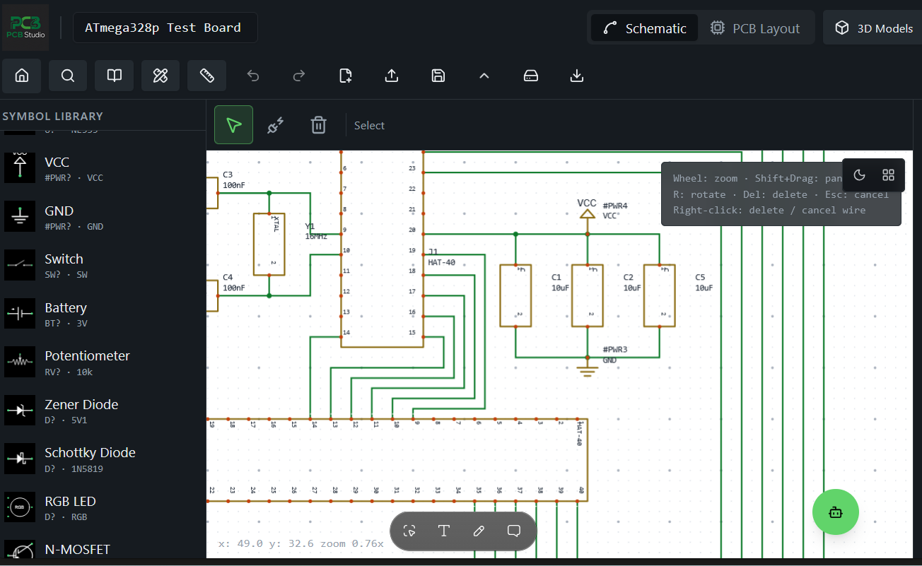
Schematic Capture
Draw circuits with a rich symbol library. Wires, buses, labels, and electrical rule checking.
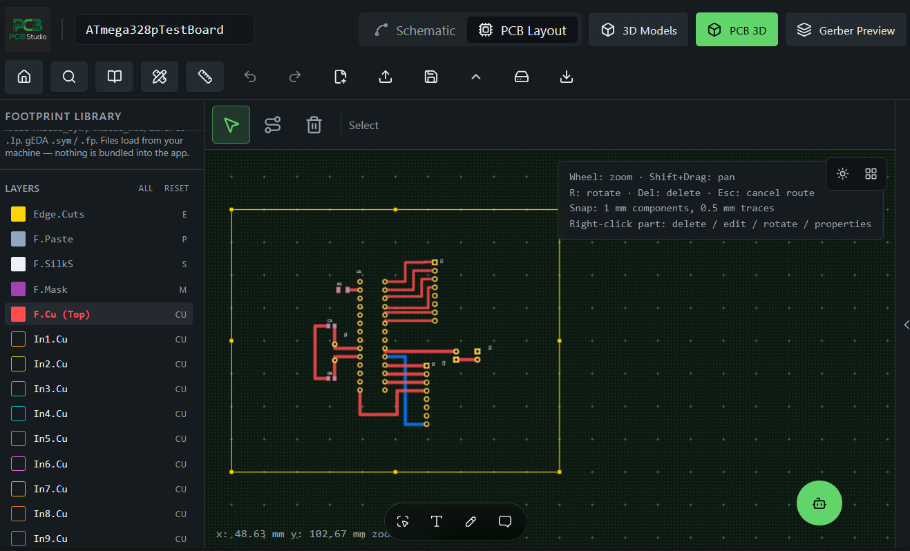
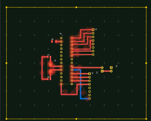
Multi‑Layer PCB Layout
Place footprints, route traces, pour copper, and manage layer stack‑ups with precision.
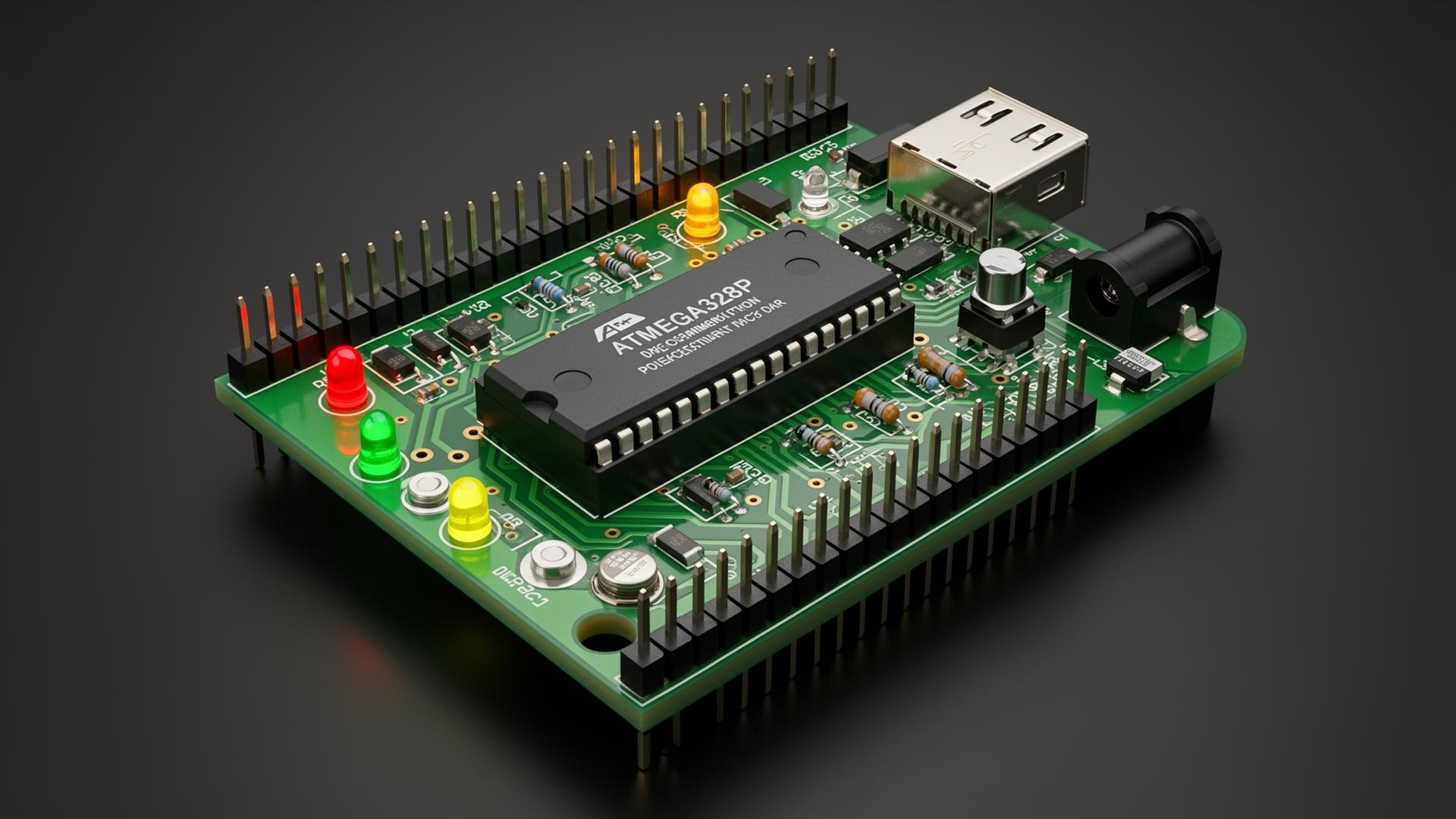
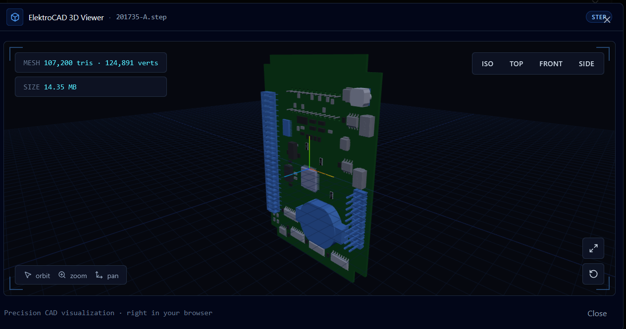
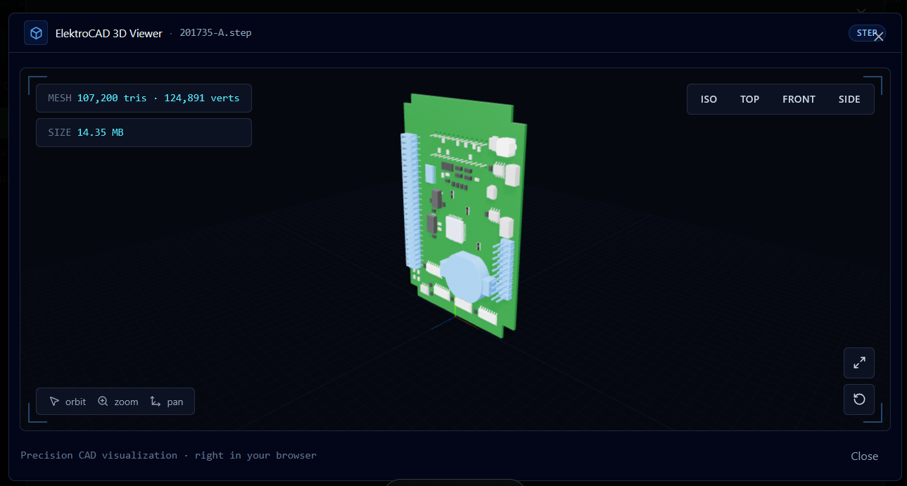
Real‑Time 3D
See your board come to life in 3D as you design — components, silkscreen, soldermask and all.
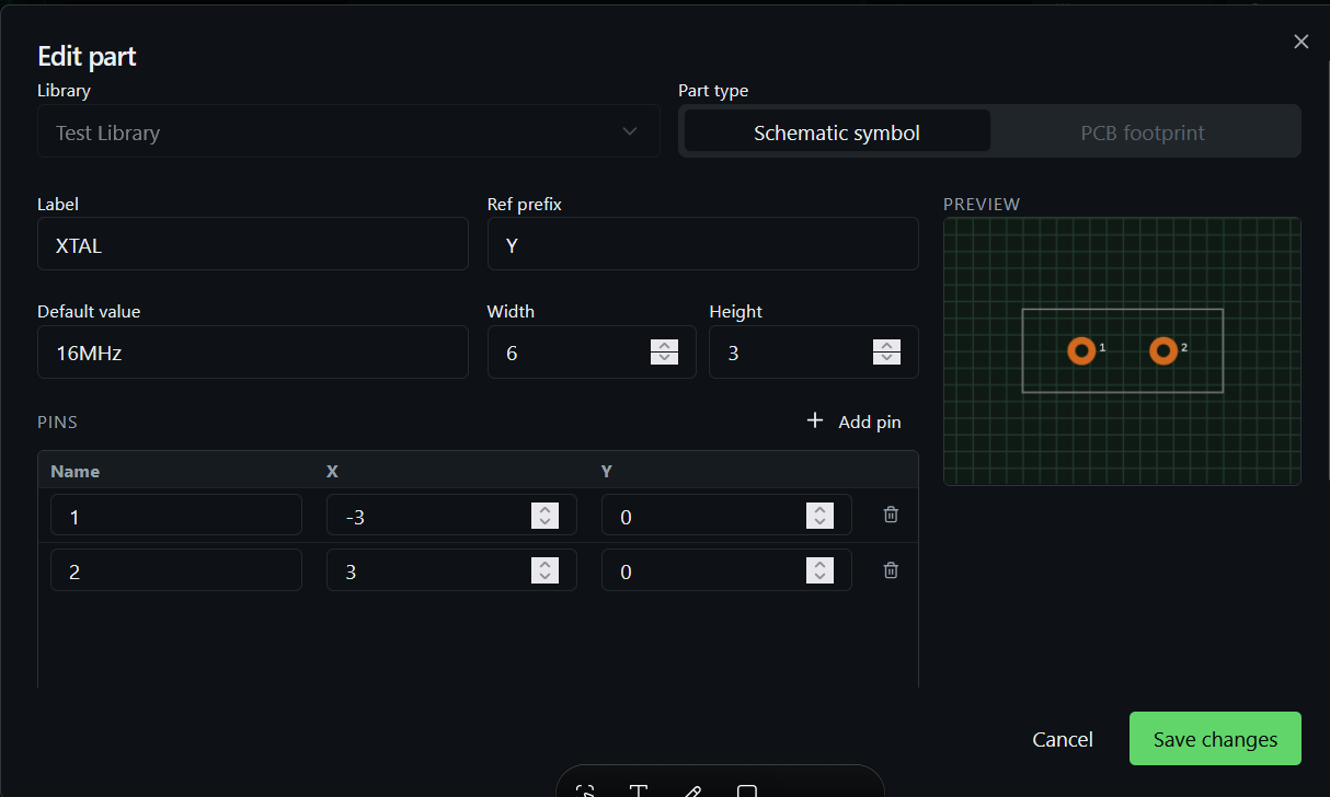
Footprint Linking
Tie footprints directly to schematic symbols so layout import is fully automatic.
Design Rule Checks
Catch clearance, width, and connectivity issues before they reach the fab house.
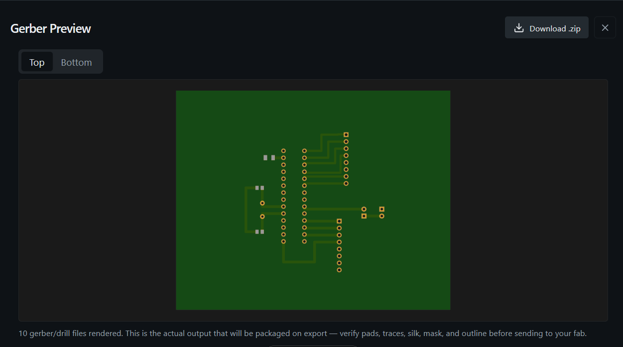
Gerber & Fab Export
Generate manufacturing‑ready outputs in seconds, ready for any PCB house.
Design your circuit, not your tool
A fast, modern schematic editor with a curated symbol library, intuitive wiring, hierarchical sheets, and instant netlist generation. Every symbol can carry its own footprint — so the jump from schematic to layout is one click away.
- Rich library of common symbols
- Per‑symbol footprint assignment
- Net labels, power symbols, and buses
- Live netlist export to PCB layout
Precision layout, without the learning curve
Place components, route traces across multiple layers, define board outlines and let live design‑rule checks keep your work fab‑ready. Import a schematic and your footprints land on the board, ready to route.
- Interactive multi‑layer routing
- Footprint library with custom pads
- Live DRC: clearance, width, connectivity
- Gerber & drill export for manufacturing
See the board before you build it
Flip between 2D and 3D instantly. Inspect component clearance, mechanical fit, and silkscreen placement in a photorealistic preview.
Schematic to layout, automatically
Every symbol carries its footprint assignment. Hit import, and parts land on the board with their nets already wired — no manual matching, no missed pads.
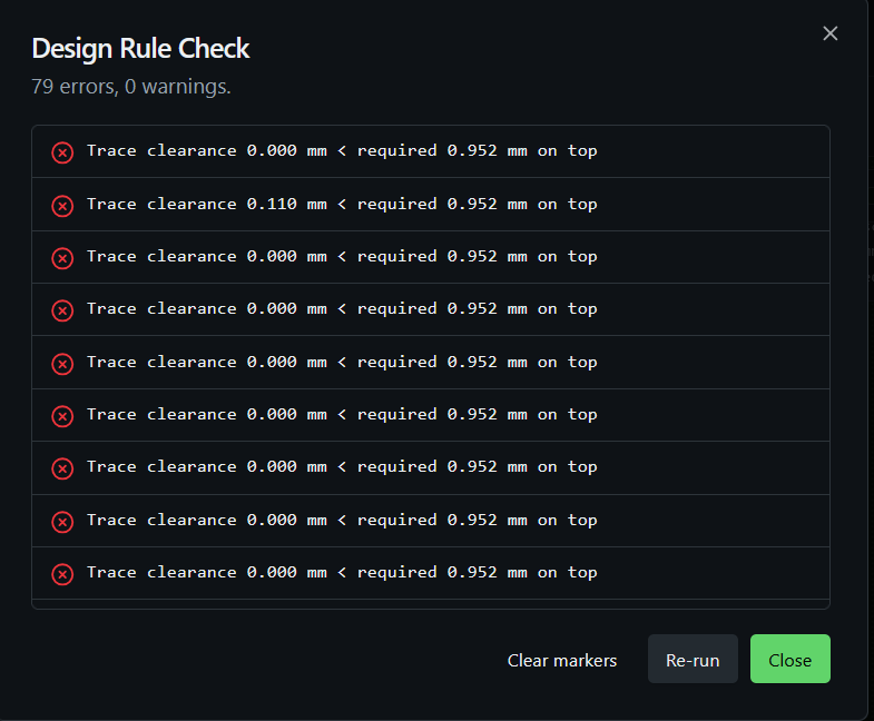
Catch issues before they reach the fab
Run DRC to flag clearance, trace‑width, drill, and body‑spacing violations against your saved design rules. Each issue is marked right on the board with a pulsing crosshair so you can find and fix it fast.
Manufacturing‑ready in one click
Export industry‑standard Gerber, drill, and pick‑and‑place files in seconds. Send the bundle straight to any PCB house.